The choice of components and the PCB footprint are interdependent. Hence, when choosing the correct component for your Rigid Flex Printed Circuit Board (PCB) or other types of PCBs, it is important to take the PCB footprint into consideration as well.
What are Footprints?
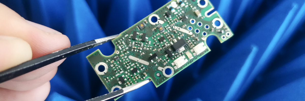
A footprint is the basic layout of the PCB. It includes the electrical and mechanical connections. It will display the electrical as well as the component outlines, and the component pins that are attached to the PCB. The footprint of both sides of a PCB should be considered.
How to Accommodate Your Components in the PCB Footprint
- For a nascent understanding of the component placement, consider drawing a basic PCB outline and mapping all the components on the PCB. Ensure that you use the actual, or scaled down measurements of the components and the board to get a clear understanding of the size and type of components you can use. Some software will even allow you to view the layout in 3-D.
- Some parts might face height restrictions. Consider the height clearance when selecting a component.
- When picking the components and designing the footprint, consider how the manufacturing process will take place. Here, you should consider the optimum soldering process (whether the manufacturer will use reflow soldering, or wave soldering).
- The components will have to be chosen and aligned according to the component affixing process.
- You can custom design the footprint according to your application, if a suitable prototype is not available.
Speak to your manufacturer about your design options. This will help you in making decisions with an experienced designer by your side. Always remember, the component choices will vary throughout the design process. Many changes will occur once the Flex PCB prototype is developed. Perfecting your PCB is a process. Take into consideration all the above factors to create a well-functioning PCB.
