PCB inspection is the fundamental quality control process that determines the electrical integrity and physical reliability of printed circuit boards before they reach end applications. Modern electronic devices demand exceptional precision, making inspection protocols essential for identifying defects such as soldering irregularities, component misplacement, and structural imperfections that could lead to catastrophic system failures.
Quality inspection significantly reduces field failure rates, minimizes warranty costs, and protects brand reputation by ensuring each board meets stringent industry standards. Advanced inspection technologies can detect microscopic defects invisible in visual inspections, providing comprehensive coverage across dense component layouts and complex geometries. This post explores PCB inspection methods, step by step, its significance, and the technological advancements in PCB inspection that enable manufacturers to achieve unprecedented quality levels.
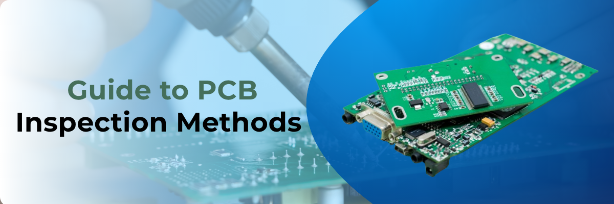
Step-by-Step PCB Inspection Methods
PCB inspection encompasses various techniques to detect issues at different production stages. Each method offers unique capabilities suited to specific defect types, from surface anomalies to internal flaws. Here are some commonly used inspection methods along with brief steps.
- Automated Optical Inspection (AOI): Begin by positioning the PCB under high-resolution cameras that capture images from multiple angles. Next, software compares these images against a reference design file to flag discrepancies in component alignment or solder quality. Finally, operators review highlighted defects for confirmation, allowing quick corrections before further assembly.
- X-Ray Inspection (AXI): Start with aligning the board in an X-ray machine to penetrate layers without damage. Then, generate cross-sectional images to reveal hidden voids, bridges, or misalignments in ball grid arrays (BGAs). Conclude by analyzing data for quantitative measurements, ensuring non-destructive evaluation of dense assemblies.
- In-Circuit Testing (ICT): Initiate by connecting the PCB to a bed-of-nails fixture that probes individual components. Proceed to apply electrical signals and measure responses for shorts, opens, or incorrect values. Wrap up with diagnostic reports that pinpoint faulty elements, ideal for high-volume production verification.
- Solder Paste Inspection (SPI): Commence by scanning the board post-paste application using laser or camera systems to assess volume and height. Follow by comparing results to tolerances for excess or insufficient paste. End with adjustments to stencil printing, preventing soldering defects downstream.
- Flying Probe Testing: Open by programming probes to move dynamically across the board without fixtures. Continue by testing electrical continuity and resistance at key points. Finish with detailed logs of anomalies, suitable for prototypes or low-volume runs.
- Functional Circuit Testing (FCT): Launch by powering the assembled PCB in a simulated environment mimicking real use. Advance to running operational sequences to check overall performance. Terminate with pass/fail criteria based on outputs, confirming system-level reliability.
- Manual Visual Inspection: Trained technicians examine boards using magnification equipment to identify cosmetic defects, component orientation issues, and anomalies that automated systems might overlook during routine inspection cycles.
Why PCB Inspection is Critical for Quality and Reliability?
Effective PCB inspection forms the core in maintaining and ensuring the quality of electronics production, directly influencing outcomes. It addresses potential problems proactively, supporting consistent results across batches. Here are some pointers that highlight its significance.
- Defect Detection Early On: Spot issues such as component shifts or poor soldering during manufacturing to avoid progression to later stages. This minimizes material waste and labor hours spent on fixes. As a result, production efficiency rises, keeping timelines intact.
- Quality Compliance: Inspection helps align with industry norms such as IPC standards through systematic checks. It verify that boards meet specifications for electrical and mechanical properties. Consequently, products gain certification, easing market entry and customer acceptance.
- Reliability in Operation: Inspection identifies weaknesses that could cause failures under stress, such as thermal cycling or vibration. It ensures components function as intended over the product’s lifespan. This builds durability, reducing field returns and enhancing brand reputation.
- Cost Reduction Strategies: It catch errors before assembly completion to lower rework expenses and prevents expensive recalls by confirming board integrity upfront. Overall, it optimizes resource use, boosting profitability in competitive sectors.
- Safety and Performance Guarantee: It detects hazards such as short circuits that might lead to overheating or malfunctions. It validates that critical applications in medical or automotive fields perform safely. Thus, it protects users and upholds ethical manufacturing practices.
- Process Improvement Feedback: Gathered data from inspections to is used to refine design and fabrication techniques. It is also used to analyze trends in defects to adjust parameters such as solder temperature. This iterative approach elevates future output standards.
- Customer Satisfaction Boost: Inspection helps deliver defect-free boards that integrate seamlessly into final devices. In turn, it fosters repeat business and positive referrals.
Technological Advancements in PCB Inspection
Innovations in PCB inspection continue to evolve, integrating new tools for precision. These developments address growing demands for speed and accuracy in complex boards.
- Artificial Intelligence Integration: Machine learning algorithms analyze inspection data patterns to improve defect recognition accuracy over time, reducing false positives and enhancing detection of subtle anomalies that traditional rule-based systems might miss.
- 3D Inspection Capabilities: Advanced optical systems capture three-dimensional surface profiles to measure component height, coplanarity, and volume parameters with precision that exceeds traditional two-dimensional imaging limitations significantly.
- High-Speed Processing: Modern inspection equipment process large amounts of image data rapidly using parallel processing architectures, enabling real-time quality feedback. This can be achieved without slowing production line throughput or creating manufacturing bottlenecks.
- Multi-Spectral Imaging: Different light wavelengths reveal various material properties and defect types, providing enhanced contrast for difficult-to-detect issues such as flux residues, contamination, and subtle color variations in components.
- Automated Programming: Inspection systems automatically generate test programs from CAD data, reducing setup time and eliminating human programming errors that could compromise inspection coverage or create false failure conditions.
- Cloud-Based Analytics: Connected inspection systems upload data to cloud platforms for advanced analytics, enabling predictive maintenance, process optimization, and quality trend analysis across multiple production facilities simultaneously.
- Integration Capabilities: Modern systems seamlessly integrate with manufacturing execution systems (MES) and enterprise resource planning (ERP) platforms, providing real-time quality data for production control and business intelligence applications.
PCB inspection is a vital process in ensuring the reliability, quality, and performance of electronic devices. Through techniques like AOI, X-Ray, and ICT, manufacturers can identify defects early in the production process, saving time and costs while ensuring the final product meets strict quality standards.
At Rigiflex Technology, we offer advanced PCB inspection solutions designed to meet the growing needs of the electronics industry. Contact us today to learn how we can help you maintain the highest standards of quality in your PCB assemblies.
