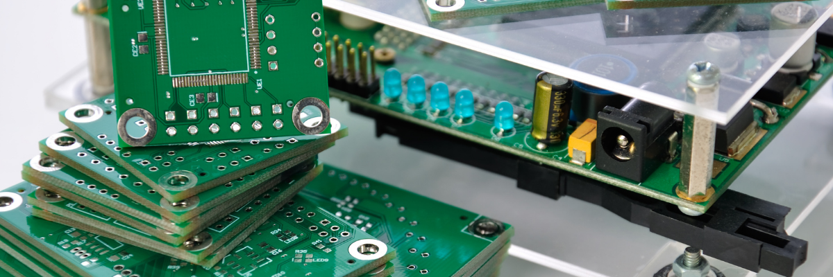
In recent years, the electronic industry has been witnessing massive improvement in the complex structures and functions of electronic devices. As the demand for miniature, faster, and powerful devices is growing, the multi-layer PCB fabrication process has gained huge traction as PCBs are becoming more and more layered and complex with an increasing number of components mounted on them. Today, almost every industrial electronic circuit comprises multi-layer PCBs. The overall functionality of these devices relies on the operation, accuracy, and design of these PCBs. Therefore, these PCBs must be designed to be functionally accurate. Despite the importance of multi-layer PCBs in modern electronics, there are chances that OEMs may make common mistakes during the fabrication of multi-layer PCBs. Would you like to know what mistakes to avoid during the multilayer PCB fabrication process? This post guides you through all of it. So, stay tuned.
Multi-Layer PCB Fabrication Process: Problems and Their Solutions Analyzed
Here is the list of common problems to avoid while manufacturing multi-layer PCBs. Let’s have a look at it.
- Design Structure: Multiple layers add an inherent complexity to the design. The risk of bows and twists is high in a multi-layer PCB manufacturing process. These two are important characteristics that determine the flatness of the circuit boards. The bow is a spherical curve of the circuit board, while the twist is a deformation that lies parallel to the diagonal of the board. PCB manufacturers should take a few steps to avoid instances of bow and twist. First, they need to select the proper parameters to reduce the stress of circuit boards. Second, it is important to select RoHS compliant materials depending upon the requirement. OEMs should be extra attentive while mixing the materials to avoid bows and twists on the circuit boards.
- Substrate Material Selection: Material selection is of the utmost important step in PCB manufacturing as it serves two essential purposes. First, circuit board materials conduct electricity, and second, they provide insulation between the conductive copper layers. As the majority of PCBs functions are determined by the substrate material, their dielectric constant should be small and stable. The smaller the dielectric constant, the smaller the signal loss will be. Additionally, substrate materials for high-frequency and high-speed PCBs should have low hygroscopicity. FR4 is one of the most popular substrate materials that have high dielectric strength.
- Resin-plugged Through Manufacturing: Resin plugging is one standardized process in the PCB industry, utilized for high-frequency and high-speed products that require large thicknesses and higher layers. It is a great alternative to the pressure-filling or green oil plugging resins method. During the multi-layer PCB fabrication process, resin plugging is one common problem a majority of OEMs face. It is a preventative measure that secures the vias from the unwanted flow of solder material. Resin plugging can be solved by using a vacuum plug machine. Initially, the resin is used to clasp the fibers together and protect them from several other factors.
- Heat Dissipation: Heat dissipation is essential and must be achieved to prevent overheating. However, OEMs face this issue during the multi-layer PCB fabrication process. Thankfully, there are different ways to facilitate minimizing or reducing the temperature of electronic components, from convective and conductive heat removal in vacuum to the use of fans and cooling radiators, and more. One of the most efficient methods for the removal of heat is using materials with a high degree of heat transfer, such as aluminum, copper, magnesium, and so on.
- Back Drilling: Back drilling is one of the most popular PCB manufacturing techniques. When it comes to multi-layer PCB fabrication, some possible issues will occur, such as hole blocking, loss of circulation, barite sag, shale instability, and many more. The right angle and manufacturing parameters should be picked to eliminate hole burr.
The pointers in this post may be useful to avoid mistakes during the multi-layer PCB fabrication process. A standardized manufacturing process guarantees a reliable, performance-driven, and economical multi-layer PCB. If you are looking for an industry player who will offer you the best PCB solutions, then Rigiflex Technology is the right choice for you. The company offers customized as well as end-to-end PCB solutions.
