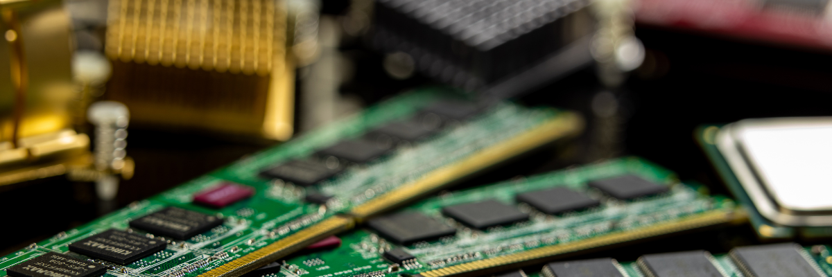
With the increasing use of microelectronics and complex circuits in PCB assemblies, the demand for 16-layer printed circuit boards (PCBs) has increased. They are found in advanced electronics as they improve signal integrity and routing and accommodate more components. They offer flexibility and high performance and are widely used in high-speed and high-frequency applications. These PCBs consist of 16 stacked layers and are vital for powering technology in many industries. This post dives into the details and advantages of 16-layer PCBs in modern electronics.
- These PCBs are made using halogen-free materials like aluminum, FR4, and CEM, thus boosting versatility and performance.
- These PCBs have a board thickness of up to 7 mm and a maximum finished size of 500 x 500 mm, providing ample space for accommodating numerous components and intricate circuitry.
- A critical part of a 16-layer PCB is the prepreg sheets. These sheets serve as insulation between the layers of copper foil. Made from fiberglass cloth coated with resin, prepreg helps prevent signal interference between nearby layers.
- Copper foil sheets are the outer layers of a 16-layer PCB stack. They carry signals and power, connecting components and directing signals between the PCB layers.
Benefits Offered by 16-layered PCBs
Here are some advantages of 16-layered PCBs:
- High signal integrity: The multiple layers allow for optimized routing and dedicated ground and power planes, which significantly reduces noise and signal losses.
- Compact design: With stacked layers, designers can fit a greater number of components in compact spaces, which makes it suitable in miniature devices and high-density applications such as network servers, aerospace, and more.
- Improved EMI shielding: The extra layers beyond ten improve EMI shielding as also the ground and power planes that help reduce noise. This helps meet regulatory compliance requirements.
- Thermal management: The PCB design in these stacked layers can accommodate enough heat sinks and ventilation, which improves heat dissipation. This makes it suitable in heat-generating applications.
- Improved power distribution: With dedicated layers for power and ground, 16-layer PCBs provide stable power delivery, reducing voltage drops and supporting high-speed performance.
Manufacturing Guidelines for 16-Layer PCBs
In multilayer PCBs, there are stringent hole-to-line requirements for hole position tolerances and inter-layer alignment tolerances. Hence, getting the aperture sizes and tolerances right is crucial for these PCBs to be a part of complex and highly dense electronic designs. A typical 16-layer PCB stackup includes multiple routing, power, and ground layers to enable improved thermal management and electrical performance. Here are some pointers for layer planning of 16-layer PCBs.
- Splitting the layers evenly and symmetrically between the top and bottom ensures proper alignment and prevents warping.
- Positioning the ground layer on the outer part of the boards improves heat dissipation and eases signal routing.
- At least 20% of the layers must be dedicated to ground and power distribution.
- Placing ground and power layers adjacent to signal layers helps decouple and control impedance.
- Split power planes should be defined to isolate different power domains, such as analog, digital, and high-current.
Applications of 16-layered PCBs
These multilayered PCBs find use in a wide range of high-tech industries and specialized fields because of their advanced capabilities and versatile design. Here are some application areas.
- Industrial Control: These PCBs are used in industrial control systems to monitor and manage different processes and machines efficiently and precisely.
- Satellite systems: 16-layer PCBs are important parts of satellite systems. They help ensure reliable communication and data transmission in space.
- Telecommunication: They are important for cell phone repeaters and communication systems and help improve signal transmission.
- Computer systems: 16-layer PCBs are essential for computer systems, including file servers used for storing and processing data. They help ensure the system runs smoothly and reliably.
- Test equipment: These PCBs are used in laboratory test equipment. They help scientists make accurate measurements and analyze results for research and experiments.
- Metrological department: Meteorological departments use 16-layer PCBs in weather analysis systems to monitor and forecast weather patterns.
- Atomic accelerators: These PCBs are important parts of atomic accelerators. They help scientists study particle physics and conduct essential scientific research.
Looking for a PCB manufacturing partner? At Rigiflex, we specialize in providing custom multilayer PCB solutions. Visit Rigiflex today to learn more about our offerings and how we can help bring your innovations to life. Reach out now to get started with your custom PCB design!
