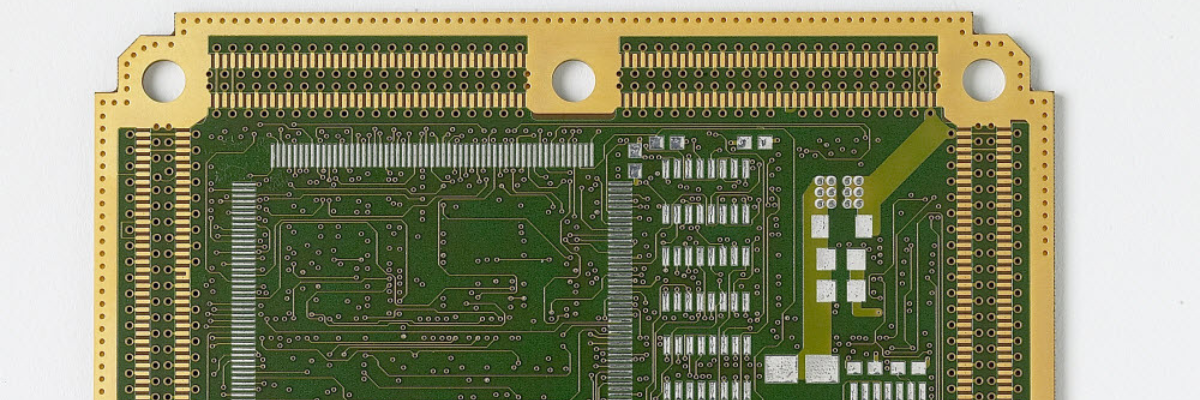
PCB gold fingers are gold-plated connecting points placed on the edge of printed circuit boards (PCBs), used for smooth, low-resistance connections in high-reliability applications. This ensures stable signal strength, durability, and conductivity. These are shiny contact pads that serve as durable, highly conductive connection points, allowing the board to plug into a connector for signal and data transfer, resisting corrosion and wear from frequent insertions.
This post explores everything you need to know about PCB gold fingers. From understanding the different types, the manufacturing process, to their benefits and applications, it covers the essential aspects.
Types of PCB Gold Fingers Based on Plating MethodsGold fingers on a PCB are typically categorized based on the method used to plate the gold. The plating method directly affects the durability and performance of the gold fingers. Below are the two most common types of gold fingers used in PCBs.
- Gold Finger with Hard Gold Plating: It is often used for PCBs that require excellent durability and resistance to wear and tear. This method involves electroplating a thicker layer of gold onto the copper surface, which makes it more resistant to abrasion. Hard gold is commonly used in applications where the gold fingers need to endure repeated mating and un-mating cycles without degrading.
- Gold Finger with Soft Gold Plating: It is used for applications where a more delicate and flexible connection is needed. Soft gold is typically electroplated with a thinner gold layer, making it easier to make initial connections with the external device. However, it is less durable than hard gold and not suitable for applications where the gold fingers will be frequently mated or unmated.
How Are PCB Gold Fingers Manufactured?
Below is a detailed and accurate breakdown of how gold fingers are made, based on standard industry practices.
- Surface Preparation and Cleaning: First, the copper pads at the PCB edge (where gold fingers will form) are thoroughly cleaned. This involves removing oxidation, oil, or other contaminants that might impair plating adhesion. Often an acid or alkaline cleaning bath is used, followed by rinsing with deionized water. After cleaning, the surface must be uniform and oxide‑free, ensuring a good foundation for the subsequent plating layers.
- Nickel Undercoat (Barrier Layer) Plating: A layer of nickel is plated over the cleaned copper pads. This nickel layer serves as a barrier to prevent copper diffusion into the gold, which might degrade conductivity or compromise reliability. It also gives mechanical support.
- Activation: After nickel plating, the surface may be treated either with a mild acid rinse or a specialized activation solution to ensure good adhesion before gold deposition. This helps avoid peeling or poor bonding between nickel and gold.
- Gold (Hard‑Gold) Electroplating on Nickel: The core gold finger plating typically involves electroplating a hard gold alloy onto the nickel undercoat. The PCB acts as the cathode and a gold anode supplies gold ions during the process. The gold alloy may include small amounts of cobalt or nickel ( 0.1–0.3%) to improve wear resistance and hardness.
- Selective Masking: Since only the edge fingers require gold plating, the rest of the PCB surface is masked off before plating. After plating, this mask or resist is removed, and the board may return to the normal manufacturing flow.
- Beveling / Edge Shaping of Gold Fingers: Once the plating is done, the edge of the PCB (where the gold fingers are positioned) is often beveled or chamfered to form a sloped shape. This makes it easier to insert the PCB into a slot or socket, reduces mechanical stress on both PCB and slot, and helps ensure consistent connections.
- Rinsing, Drying and Cleaning After Plating: After gold plating, the board is rinsed (often with deionized water) to remove residual plating solution or chemicals. Proper drying ensures no residues remain.
- Final Inspection and Quality Control: Every board must be inspected after plating for thickness uniformity, adhesion, surface defects, and to verify that plating stayed only on desired areas.
Benefits of PCB Gold Fingers
Gold fingers offer several advantages that make them significant in PCB designs. Some key benefits include:
- Durability: Gold is resistant to corrosion and oxidation. This makes gold fingers an ideal choice for connectors that need to endure harsh environmental conditions.
- Low Contact Resistance: Gold has excellent conductivity, which means gold fingers offer minimal resistance at the contact points, ensuring efficient signal transmission.
- Wear Resistance: Gold fingers are resistant to wear, making them ideal for connectors that will undergo frequent mating and un-mating, such as in computer hardware or telecommunications equipment.
- Enhanced Reliability: The robustness of gold fingers helps ensure that connections remain reliable over time, minimizing the risk of failures in critical electronic systems.
Key Design Requirements for PCB Gold Fingers
When designing PCBs with gold fingers, it’s important to consider the following requirements:
- Plating Thickness: The thickness of the gold plating must be appropriate for the intended use. For high-performance applications, thicker plating may be necessary to ensure durability and reliability.
- Edge Design: The edges of the gold fingers must be carefully shaped to ensure proper mating with connectors. Sharp edges or irregular shapes can lead to poor connection quality.
- Solderability: The gold fingers must be designed for optimal soldering. This requires careful consideration of the surface finish to ensure that the solder adheres properly.
- Environmental Factors: The design should take into account the environmental conditions the PCB will be exposed to, including temperature variations, humidity, and exposure to chemicals.
Applications of PCB Gold Fingers
Gold fingers are used in a variety of applications across different industries. Some common uses include:
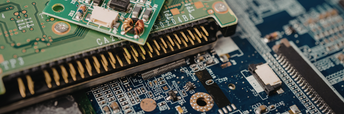
- Computer Memory Modules: The most common application is in RAM modules (DDR4, DDR5, SODIMM). Memory sticks slide into motherboard slots and rely on gold fingers for high-speed data transfer.
- Graphics and Video Cards: GPUs and dedicated graphics cards use gold fingers to connect to PCIe slots on motherboards. The gold plating ensures stable power delivery and high-bandwidth data transmission critical for graphics processing.
- Expansion Cards: Various expansion cards utilize gold fingers. These include sound cards, network interface cards (NICs), Wi-Fi adapters, capture cards, RAID controllers, and USB/Thunderbolt expansion cards.
- Industrial and Embedded Systems: Modular industrial systems use gold fingers for Programmable Logic Controller (PLC) modules, backplane systems where multiple cards connect to a central board, instrumentation modules in test equipment, and automation control cards.
- Telecommunications Equipment: Telecom infrastructure relies on gold fingers for line cards in switches and routers, signal processing modules, network interface modules, and base station equipment cards.
Common Problems in PCB Gold Fingers and How to Avoid Them
While PCB gold fingers are an excellent choice for many applications, they are not immune to issues. Here are some common problems and tips for avoiding them.
- Poor Gold Plating Quality: Insufficient gold plating or poor adhesion can lead to issues with connectivity and wear. To avoid this, ensure that the gold plating process is done under controlled conditions and that the plating thickness is within specifications.
- Wear and Tear: Over time, the gold fingers may wear down due to repeated connections. Using hard gold plating for applications with high mating cycles can help extend the life of the fingers.
- Soldering Issues: Inadequate solderability can cause problems during assembly. Ensure that the PCB design includes proper surface finishes and that the gold fingers are free from contaminants before soldering.
Whether for memory modules, expansion cards, telecom gear, or consumer electronics, PCB gold fingers help ensure stable and lasting connections. If you are looking for quality PCB manufacturing services, including rigid, flexible, or rigid‑flex PCBs with gold plating options, consider reaching out to Rigiflex Technology today.
