As the technology continues to advance, the demand for complex electronic circuits and printed circuit boards is on the rise. From smartphones to medical devices, these intricate designs require advanced PCB assembly techniques to ensure reliable and high-performance operation. The PCB assembly techniques have evolved over the years for complex circuits, which you must be aware of. This post is a must-read for you if are an electronics engineer, a PCB designer, or simply curious about the inner workings of your favorite gadgets as it lists a few of the advanced PCB techniques employed in the making of today’s complex circuits.
An Overview of the Advanced PCB Assembly Techniques
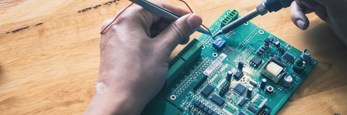
The utilization of certain PCB assembly techniques is inevitable for the successful manufacturing of complex circuits. There are several techniques used today that ensure optimal performance and reliability of the final product. A few of them include:
- Microvias Technology: Microvias are small holes drilled into the PCB substrate, enabling the interconnection of traces across various layers of the board. This advanced technique allows for the creation of complex multilayer circuits with exceptional routing density. Microvias technology requires specialized equipment and expertise to ensure proper drilling, plating, and insulation of the vias.
- Fine Pitch Component Placement: Fine pitch is the spacing between the leads or pads of surface mount components. Advanced PCB assembly techniques encompass the placement of components with pitches smaller than 0.8mm. This demands high-precision placement equipment and techniques. Proper alignment and soldering methods are also critical to prevent misalignment or solder bridging.
- Controlled Impedance Routing: Controlled impedance is one of the major aspects of PCB design that involves the precise management of electrical characteristics in traces and transmission lines. This technique is employed to achieve optimal signal integrity and minimize electromagnetic interference (EMI) in high-speed circuits. It is important to determine trace width and spacing carefully, along with choosing the appropriate dielectric material to attain controlled impedance routing. This advanced approach plays an important role in ensuring reliable performance and mitigating potential issues that may arise from unstable signal transmission.
- Advanced Soldering Techniques: High-level PCB assembly techniques incorporate advanced soldering methods like reflow soldering or wave soldering, which guarantee reliable and uniform solder joints for surface mount components. Furthermore, specialized techniques like solder jetting or selective soldering may be employed for specific components or applications.
- Conformal Coating: The application of conformal coating to a fully assembled printed circuit board is one of the best ways to safeguard the board against various environmental elements, including moisture, dust, and chemicals. This protective layer significantly enhances the stability and durability of the circuit, ensuring its long-lasting performance. The process of applying conformal coating demands attention to detail to ensure complete coverage without compromising electrical connectivity.
- Multi-Board Stackup Design: It involves the arrangement and connection of multiple circuit boards to create a single system or device. This method is frequently utilized in applications that demand advanced performance and intricate capabilities. Through meticulous stackup design, engineers can reduce signal interference, enhance power distribution, and establish effective thermal management within the system.
- EMI/EMC Shielding: Electromagnetic interference (EMI) and electromagnetic compatibility (EMC) are terms used to describe the undesirable radiation that can interfere with the functioning of electronic devices. In today’s PCB manufacturing, several advanced types of shielding techniques are employed like board level shielding to safeguard sensitive components against external sources of EMI or prevent the circuit from emitting EMI. These methods are extremely important in applications where regulatory standards for electromagnetic compatibility must be met.
All these advanced PCB assembly techniques demand expert knowledge and experience in circuit design and manufacturing. These techniques involve intricate processes and components that require a high level of expertise and precision. To ensure the successful implementation of advanced PCB assembly techniques, it is necessary to associate with leading PCB manufacturers in the marketplace like Rigiflex, who possess the necessary skills and experience in circuit design and manufacturing using modern techniques. Their expertise will guarantee the highest quality and efficiency in the assembly process, resulting in superior performance and reliability of complex circuits
