Electronics technology has made many advances in the last few decades. One of the advancements has been the reduction in the sizes of computers, cell phones, and video cameras. High Density Circuit (HDI) Printed Circuit Boards (PCBs) are the reason behind this advancement. How does HDI technology contribute to the performance and popularity of these products? We answer this question in this post.
A Few Benefits of HDI PCB Capabilities
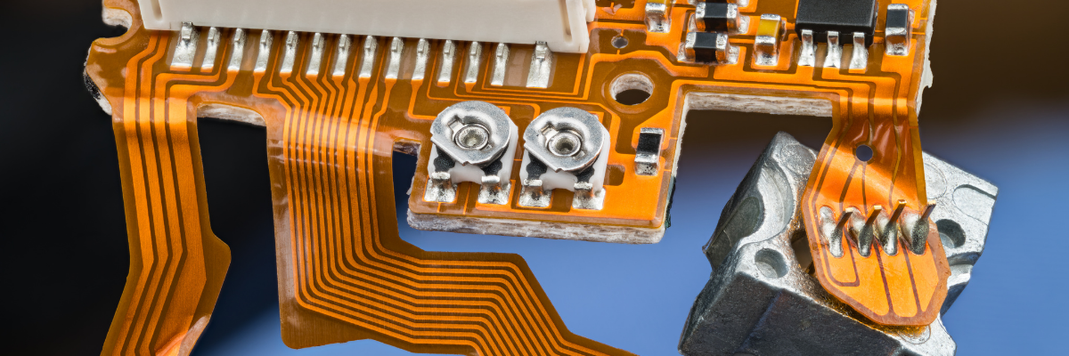
The reason that electronic devices are becoming smaller in size is because of the use of certain processes and technologies. These technological solutions are making it easier for designers to create PCBs that can help in faster product manufacturing, and meeting customer requirements.
Via in Pad Process for Better PCB Production: This process was inspired by SMT technology. The via in pad process allows vias to be placed inside the circuit board’s flat lands. The vias can be either plated or filled with epoxy, and then capped. These two steps not only make the vias invisible, but also eliminates eight steps of the HDI PCB production process. For this reason, the via in pad process is always used for creating PCBs with Ball Gird Arrays (BGA), Chips on Boards (COB) and Chip Scale Packages (CSP).
Cost-Effective Designs: Even though electronic products are manufactured in smaller sizes, customers still expect the products to have high quality performance. When HDI technology is used in PCB design, it allows the designers to reduce the size of the PCB from 8 layers to 4 layers. Also, the wiring of the 4 layered PCB can be designed as such that it will function the same as an 8 layer Flex PCB. The reduction layer count also leads to reduction in usage of manufacturing materials. These aspects affect the overall price of the electronic product, making it a value for money purchase for the customer.
Multiple via Processes for Increased Performance: As most PCBs used in electronic products are double sided and multi-layered, multiple via processes are used in the PCB manufacturing process. The use of blind via, or via in pad technology enables designer to place small sized components closer together on the board. This leads to PCBs with smaller pitches and I/O geometries. As a result, the PCBs are able to transmit signals faster, without suffering from crossing delays, or signal losses.
The above points are just a few examples of how HDI PCB technologies are driving the performance and popularity of electronic products. The changing needs of customers will drive HDI PCB Capabilities ahead, and help PCB manufacturers to come up with better products in the future.
