When printed circuit boards (PCBs) are discussed, the first thought that comes to mind is their contribution to the advancements in electronics and their implementation across industries. PCBs are the core or backbone of several modern handheld gadgets, industrial machines, devices, and integrated systems. Amid all the components, circuits, and wiring, the bare printed circuit board forms the fundamental core on which the entire circuit is assembled. So, why are bare boards so significant? Would you like to know more about them? If yes, read this post till the end.
What Are Bare PCBs?
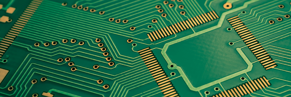
Bare printed circuit boards (PCBs) act as the base of an electronic device. They don’t have any components soldered onto them. Instead, they provide the foundation for components to be strategically positioned and connected, creating the intricate network of circuits that make devices function. Every pathway, electrical connection, and interaction between components begins with the design and layout of the bare printed circuit boards.
How Are Bare PCBs Manufactured?
Manufacturing bare printed circuit boards involves several processes, requiring attention to detail, precision, and advanced manufacturing techniques. Here is a quick overview of the process.
- Design and Layout: This is the first and the most important step. Engineers design the circuit layout using specialized software that helps determine the placement of traces, components, vias, and more.
- Substrate Selection: The selection of substrate material is another crucial step. Typical substrate materials used for bare PCBs include fiberglass-reinforced epoxy resin, which provides rigidity and insulation. Aside from that boards may be made of aluminum, plastic, and so on.
- Copper Cladding: This is the foundational process in bare circuit board manufacturing. The purpose of copper cladding is twofold. First, it involves the application of thin layers of copper onto the substrate material. The copper coating forms the conductive pathways allowing electrical signals and power to flow through the circuit. Secondly, it sets the stage for processes such as etching and photoresist applications, which define the final circuit layout.
- Photoresist and Etching: The combination of photoresist and etching enables the precise definition of pathways on the bare circuit boards. This allows for the creation of intricate designs with high precision and repeatability.
- Solder Mask Application: A protective layer known as a solder mask or solder resist is applied to the board’s surface. This layer serves multiple purposes vital to electronic devices’ functionality, reliability, and assembly. It encapsulates copper traces, prevents solder bridges, aids in component placement, and contributes to the overall quality of electronic devices by protecting the vital circuitry from environmental and assembly-related challenges.
- Silkscreen Printing: It involves the detailed markings and identifiers on the surface of the PCB. This step adds essential visual and informational elements to the circuit board, aiding in component identification, assembly, testing, and overall functionality.
- Testing and Quality Control: Before being assembled, every bare PCB undergoes rigorous testing to ensure the structural integrity and possible issues in the layout.
Significance of Bare PCBs
Some OEMs may choose to source bare PCBs from a board manufacturer and assemble them separately for various reasons. Here are some reasons why bare PCBs may be significant.
- Customization: These PCBs allow for complete customization of circuit layouts to suit specific electronic applications. Designers can create intricate patterns of traces and components to meet the desired functionality and performance requirements.
- Compactness: You can get base boards manufactured based on your required size and shape. This allows the precise arrangement of components and traces. This is especially important for portable devices, wearables, and miniaturized electronics.
- Cost-Effectiveness: Manufacturing bare PCBs can be more cost-effective than producing completely assembled ones. The initial investment in the fabrication of bare boards is often lower, and bulk production can lead to economies of scale.
- Versatility: They can be customized to make assemblies for various industries from consumer electronics and medical devices to telecommunications and aerospace technology. Their versatility makes them suitable for a wide range of electronic products.
- Prototype Development: Bare PCBs are ideal for product development and prototyping before moving to full-scale production. Extra bare PCBs can become an easy replacement in case of any PCBA issue. They allow designers to refine their concepts and experiment.
- Rapid Manufacturing: Bare board manufacturing has become more streamlined and efficient. This allows for quicker turnaround times in production. This is useful for industries with short product lifecycles.
- Advanced Technologies: Bare PCBs, depending on their materials, can easily incorporate advanced technologies such as high-density interconnect (HDI) techniques, allowing for improved signal integrity and greater miniaturization in high-performance microelectronics.
If you are an OEM that needs assembly in your devices, consider sourcing bare boards and experimenting with the design and layout. Consulting an industry player like Rigiflex Technology is always a good practice if your next electronic application demands bare boards for prototyping. With years of market presence, the company offers PCB services considering your application need. Their team of experts will assist you if you have any queries or doubts about bare PCBs and their application.
