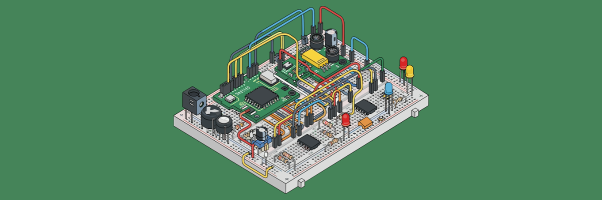
PCB layout design is important in electronics manufacturing because it bridges the gap between concept and reality. Converting schematics into a physical PCB involves meticulous planning of components, traces, layers, vias, and power/ground planes.
Each element must work in harmony to ensure signal integrity, thermal efficiency, and manufacturability. The layout determines how well your circuit performs under real-world conditions. Poor design choices lead to signal loss, electromagnetic interference, and thermal failures. Getting it right means understanding electrical principles, manufacturing constraints, and material properties.
Step-by-Step PCB Layout Process Explanation
The PCB layout process follows a structured approach that transforms your schematic into a manufacturable board design, ensuring every connection meets electrical and mechanical requirements.
- Schematic to Board Setup: Importing the netlist transfers all connections from your schematic into the layout software, establishing the foundation for your physical design. Defining board size and shape considers mechanical constraints, enclosure fit, and connector placement to match your application requirements.
- Component Placement: Positioning key components for signal flow requires understanding of how signals travel through the circuit, minimizing path lengths for critical connections. Thermal, mechanical, and EMI considerations influence component spacing, heat sink placement, and the separation of noisy digital circuits from sensitive analog sections.
- Routing: Signal routing for critical signals and differential pairs demands careful attention to impedance matching, equal trace lengths, and controlled coupling. Power and ground routing establishes low-impedance distribution networks supplying stable voltage. Via usage connects different layers strategically while minimizing inductance and signal reflections.
- Design Rule Checks (DRC): Spacing, clearance, and trace width verification ensures your design meets electrical safety standards and prevents manufacturing defects such as open circuits. Manufacturer capability checks confirm that your design specifications align with the fabrication house’s equipment tolerances, layer capabilities, and minimum feature sizes.
- Final Output Files: Gerber files contain the copper pattern, solder mask, silkscreen, and other layer information needed for fabrication. Drill files specify hole locations, sizes, and types for vias and component mounting. BOM and assembly files guide the component procurement and board assembly process.
Key Factors That Affect PCB Performance
Several design parameters directly influence how your PCB performs in terms of signal quality, thermal behavior, and electromagnetic compatibility.
- Layer Stackup: Layer stackup arrangement determines impedance control, signal-to-ground coupling, and electromagnetic shielding effectiveness throughout your board. The sequence of signal, ground, and power layers affects crosstalk, return path quality, and manufacturing cost based on total layer count.
- Trace Width and Spacing: Trace width affects current carrying capacity, impedance matching, and manufacturing yield since narrower traces are harder to fabricate reliably. Spacing between conductors prevents voltage breakdown, reduces capacitive coupling, and maintains clearance requirements for different voltage levels across your design.
- Ground Planes and Return Path: Ground planes provide low-impedance return paths for signals, reducing loop areas that cause EMI and improving signal integrity significantly. Return path continuity ensures signals have uninterrupted ground reference beneath them, preventing discontinuities that create impedance changes and signal reflections.
- Thermal Management Basics: Thermal management involves distributing heat through copper pours, thermal vias, and strategic component placement to prevent hotspots that degrade performance. Adequate cooling paths transfer heat from power components to heat sinks or ambient air, extending component lifespan and maintaining stable operation.
Best Practices to Follow in PCB Layout Design
Following proven design techniques helps you create reliable, manufacturable PCBs that perform consistently across production runs and operating conditions.
- Placing the Component First and Route Second: Component placement establishes the physical arrangement that determines routing complexity, signal path lengths, and thermal distribution across your board. Optimizing placement before routing reduces iterations, minimizes trace crossovers, and creates cleaner layouts that are easier to manufacture and debug.
- Keep High-Speed Signals Short and Clean: High-speed signals benefit from direct, shortest-path routing that minimizes reflections, crosstalk, and timing skew between related signal groups. Clean routing avoids unnecessary vias, maintains consistent impedance, and uses appropriate termination techniques to preserve signal edge rates and amplitude.
- Avoid 90° Trace Angles: Trace angles greater than 45° cause impedance discontinuities that reflect signals, and sharp corners can trap acid during etching processes. Using 45° angles or curved traces maintains smoother impedance transitions and improves manufacturing reliability while reducing potential signal integrity issues.
- Follow DFM Rules: DFM rules specify minimum feature sizes, spacing requirements, and design constraints based on your fabricator’s equipment capabilities and process controls. Adhering to these guidelines prevents costly redesigns, improves yield rates, and ensures your boards are manufactured with the same consistency.
Common Mistakes to Avoid
Recognizing frequent layout errors helps you prevent problems that compromise board functionality, increase costs, or delay production schedules.
- Poor Grounding: Poor grounding creates ground loops, raises reference voltages unevenly, and allows noise to couple between different circuit sections. Inadequate ground connections increase return path impedance, causing signal distortion, EMI emissions, and unpredictable circuit behavior during operation.
- Incorrect Trace Widths: Incorrect trace widths either restrict current flow causing voltage drops and overheating, or waste board space with unnecessarily wide conductors. Calculating proper widths based on current requirements, temperature rise limits, and impedance targets ensures reliable operation without excessive copper usage.
- Crowded Component Placement: Crowded component placement prevents adequate cooling, complicates assembly processes, and makes rework nearly impossible when component replacement becomes necessary. Proper spacing allows airflow, accommodates manufacturing tolerances, and provides access for inspection, testing, and potential modifications after assembly.
- Ignoring Thermal Relief: Ignoring thermal relief makes soldering difficult because large copper pours quickly draw heat away from pads during assembly. Thermal relief patterns balance electrical conductivity with thermal isolation, allowing proper solder joint formation while maintaining necessary connections to planes.
Partner with Rigiflex Technology for Expert PCB Layout Design
Rigiflex Technology offers complex layouts, multilayer boards, and high-performance applications with precise PCB layout design services with customization options. Our manufacturing expertise helps your designs meet exact specifications from concept to production.
For project discussions or requirements, call (714) 688-1500 or email pcboards@rigiflex.com
FAQs
- How does PCB layout design impact product reliability over time?
PCB layout design controls heat flow, mechanical stress, and signal stability, directly affecting component lifespan, solder joint strength, and consistent electrical performance throughout prolonged operating conditions.
- Can PCB layout design reduce manufacturing costs?
An optimized PCB layout reduces routing errors, assembly rework, and scrap rates, improving fabrication yield while controlling material usage and overall manufacturing expenses.
- What role does simulation play in PCB layout design?
Simulation identifies signal integrity, thermal distribution, and power delivery risks early, allowing layout refinements before fabrication and preventing costly post-production corrections.
- Is PCB layout design different for low volume and high-volume production?
Yes, high volume layouts focus on yield, automation, and consistency, while low volume designs allow layout flexibility, quicker revisions, and faster design validation cycles.
- Does PCB layout design affect compliance testing results?
PCB layout design strongly influences EMI emissions and noise coupling, directly impacting whether electronic products meet regulatory standards during electromagnetic compliance testing.
