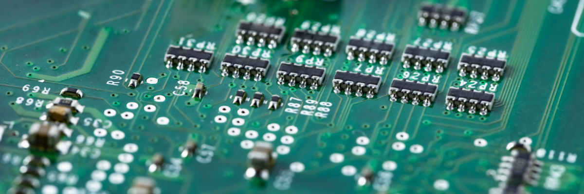
A Printed Circuit Board (PCB) is a structure used to connect and support electronic components. PCBs have conductive pathways through which different components are connected across the board. These pathways are etched from copper sheets. To ensure that the copper layer does not conduct a signal or current, it is laminated into a substrate.
Types of PCB Lamination Procedures
Following are the generally used PCB lamination processes, which are based on the type of PCBs used:
Multiple Layer PCBs: Circuit boards that are composed of various layers are known as multi-layer PCBs. These layers can be either thin etched boards or trace layers. In both cases, they are bonded with lamination. For lamination, the internal layers of the PCB are subjected to under extreme temperature (375o F) and pressure (275 to 400 psi). This procedure is implemented when laminating with a photosensitive dry resist. Later, the PCB is allowed to cure at a high temperature. Finally, the pressure is slowly released and the lamination material is slowly cooled.
Double-sided PCBs: Although, the manufacturing aspects of double-sided PCBs are different from other types of PCBs, the lamination process is quite similar. A photosensitive dry resist layer is used to laminate the PCB panel. The process is carried out under extreme temperature and pressure as mentioned in the multilayer PCB point.
Sequential Lamination: Sequential lamination technology is used if the PCB comprises two or more subsets. The subsets of the multi-layer PCBs are created in separate processes. After this, a dielectric substance is interposed between each pair of subsets. Standard manufacturing procedures are implemented after this process.
Teflon (PTFE) Microwave Laminates: PTFE microwave laminates are one of the most used laminates for PCB lamination. The reasons for this are, it has consistent dielectric constant, very low electrical loss, and tight thickness tolerance. These features are ideal printed circuit boards, which are used in applications comprising radio frequencies. CTFE (chlorotrifluoroethylene) thermoplastic film is a common material used for PTFE lamination.
Choose a suitable lamination procedure, depending on the intricacies of your application. Speaking to the manufacturer is the best solution to get answers to any queries you may have. For more information about PCB Lamination Process, please visit http://www.rigiflex.com/ or contact the company at (714) 688-1500.
