The demand for fast, performance-driven, and miniature devices has increased over the years. A large number of these products are driven by printed circuit boards (PCBs). OEMs today achieve this requirement by using fewer through-hole components. However, it is nearly impossible to allocate a huge space for large plated through-hole components and their associated lands. Here, surface-mounted components make a significant difference. As the surface mount technology becomes increasingly popular, most of the plated through-holes on the modern circuit board designs end up being vias. Vias are one of the essential parts of the multi-layered PCB design and manufacturing process. They interconnect different layers in the PCB. They are widely used in small-scale ball grid arrays (BGA) and PCBs. Would you like to know about PCB vias?
Get Introduced to PCB Vias
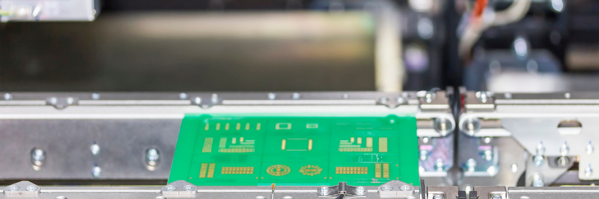
Vertical interconnect access (Vias) are plated through holes in a PCB. As the term implies, they deliver a route using which electrical and thermal energy moves in the board from one layer to another. Vias can be drilled by either laser or mechanically depending on the application requirement. Vias play a vital role in multi-layer printed circuit boards that are complex to design and manufacture.
What Are the Most Common Types of PCB Vias?
Here are some most popular types of PCB vias available today. All vias offer the same functionality, but each has the strength that enables it to make a smooth PCB assembly. So, let’s have a look at them.
- Buried Vias: This is one of the important types of PCB vias. Buried vias can be drilled mechanically. Popularly known as hidden vias, they are located in the interior region of the circuit board. Hence, there are no paths that route towards the outer layers. According to the institute for printed circuits or IPC standards, buried vias must be less than 150 micrometers in diameter.
- Blind Vias: This type of vias is drilled mechanically from either the top or bottom layer. But, it doesn’t penetrate through the entire circuit board. It is used to connect the top to the center layer and in some instances, the external layer to the adjacent layer. Once the lamination is performed, the other side of the hole cannot be seen. Thus, they are called blind vias.
- Through Vias: This is another important type of PCB vias. The holes are drilled from the top to the bottom layer. They can be either plated through-hole (PTH) or non-plated through hole. Through vias are open at both ends, enabling plating to flow through the circuit board and coat the hole to make it conductive.
Important Designing Tips When Choosing PCB Vias
The aforementioned PCB vias types have their specific functions and attributes. Therefore, which PCB vias type to choose entirely depends on the application requirement. No matter what you choose, there are certain design tips you may want to consider when employing PCB vias in your design. This section describes the same.
- Try to implement smaller via structures in your design. This helps build high-density printed circuit boards.
- The aspect ratio should be minimum for better electrical performance and signal integrity.
- Via-in-pads should be filled, unless they exist in thermal pads.
- The pad matrix should include blind vias and through vias. They must be filled and planarized, else solder joints may be compromised.
- Try to incorporate vias in thermal pads. This will help the solder flow through to the conductive planes.
- Do check for a minimum clearance of vias and traces from routed edges. Also, check for vias positions for BGA packages.
- The circuit board documentation includes a drill file with X-Y coordinates and tool codes for all holes. In addition to this, the documentation should include the GERBER files that consist of via plugging holes if required.
The aforementioned types of vias in PCBs not only increase the density but also bring down the cost in volume production. With the advancements in high-density PCB designs, their manufacturing has become relatively easy. However, requirement sharing must be accurate to get the right via type, which plays a key role. If your forthcoming electronics project involves vias and you are not sure which type to choose, then you must consult an industry player for the best solution. With reliable vias filling processes, Rigiflex Technology specializes in designing and manufacturing high-density PCBs. Their experts work closely with clients to understand their requirements.
