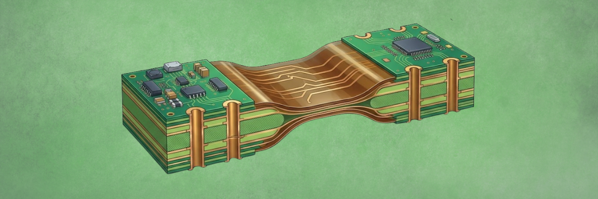
A rigid-flex PCB stackup combines rigid and flexible substrate layers within a single printed circuit board structure, enabling compact, lightweight, and highly reliable electronic designs. These hybrid PCB configurations are widely used in aerospace, medical devices, consumer electronics, automotive systems, and industrial equipment where space optimization, durability, and flexible interconnections are critical.
However, designing an effective rigid-flex PCB stackup requires careful consideration of layer configuration, bend regions, material selection, signal integrity, impedance control, and manufacturability. Poor stackup planning can lead to reliability issues, mechanical stress failures, and increased production complexity.
In this rigid-flex PCB stackup design guide, we will explore rigid-flex PCB layer stackup structures, common stackup configurations, key rigid-flex stackup design considerations, manufacturing constraints, and best practices for optimizing performance and long-term reliability.
Structure of a Rigid-Flex PCB Layer Stackup
The structure of a rigid-flex PCB stackup consists of both rigid and flexible layers, each serving distinct functions in the overall design.
Here is a detailed breakdown of the key components:
Rigid Layers:
- FR4 Core: The rigid base layer provides structural support for the PCB and allows for reliable signal transmission.
- Copper Layers: These layers carry electrical signals and are essential for the PCB’s functionality.
- Prepreg: Prepreg material serves as an adhesive layer between copper layers and other components, contributing to the rigidity of the board.
Flexible Layers:
- Polyimide Substrate: Flexible polyimide material allows for bending without compromising electrical performance.
- Thin Copper Foil: Thin copper foil on flexible layers allows for signal routing and connectivity while maintaining flexibility.
- Coverlay: Coverlay is used to protect the flexible layers, ensuring mechanical strength and providing insulation.
Transition Zones (Rigid ↔ Flex):
- Critical Stress Regions: Transition zones where the rigid and flexible parts meet are susceptible to mechanical stress. These zones must be carefully designed to prevent breakage.
- Layer Continuity and Bonding: Ensuring seamless bonding between rigid and flexible layers ensures that the final design functions optimally without signal loss or mechanical failure.
Common Rigid-Flex PCB Stackup Configurations
Rigid-flex PCB stackups come in various configurations, each suited for different design requirements. Here are some of the most common stackup designs:
- Single Flex Layer Stackup: This configuration includes a single flexible layer sandwiched between rigid sections. It is typically used in applications requiring minimal flexibility, such as portable devices.
- Double-Sided Flex Stackup: This configuration consists of two flexible layers with rigid layers on either side, allowing for more flexibility and suitable for complex designs with higher flexibility requirements.
- Multilayer Rigid-Flex Stackup: A multilayer stackup includes multiple layers of rigid and flexible materials, which are ideal for designs requiring advanced flexibility, high-density routing, and multiple electrical connections.
Key Design Considerations for Rigid-Flex PCB Layer Stackup
Designing a rigid-flex PCB stackup requires addressing various factors that significantly influence both performance and durability. Here’s a deeper look at the essential considerations:
- Layer Symmetry: Maintaining symmetry across the stackup is crucial to ensure uniform mechanical stress distribution. Asymmetry in layer thickness can lead to areas of excessive stress, especially in the bend areas, potentially causing mechanical failure or signal loss.
- Bend Area Design: The bend area in rigid-flex designs must be precisely planned to withstand mechanical stress over repeated cycles of flexing. Ensuring the proper copper thickness and avoiding sharp bends are key to preventing fractures and performance degradation over time.
- Material Selection: Choosing the right materials for both rigid and flexible layers directly impacts the overall performance of the PCB. Factors such as electrical conductivity, mechanical strength, flexibility, and thermal management should be considered for optimal performance and reliability.
- Copper Thickness Optimization: Optimizing the copper thickness in flexible layers is essential for balancing flexibility and electrical conductivity. Too thin layer may lead to signal integrity issues, while too thick may affect the flexibility of the PCB.
Manufacturing Constraints in Rigid-Flex Stackup
Rigid-flex PCB manufacturing involves a higher level of process complexity compared to standard rigid or flexible PCBs due to the integration of dissimilar materials, intricate layer structures, and controlled bending requirements. A clear understanding of these constraints is essential for developing a manufacturable and robust rigid-flex stackup design.
- Layer Registration: Accurate alignment of the rigid and flexible layers is essential for ensuring both electrical and mechanical integrity. Any misalignment during the manufacturing process can lead to poor performance, signal disruption, or potential failures.
- Lamination Cycles: Lamination cycles are crucial in ensuring proper bonding between layers. However, too many cycles can compromise the structure and lead to delamination, which negatively affects the PCB’s durability and performance. Proper cycle control is necessary for consistent, reliable manufacturing.
- Yield Impact: Due to the intricacies of rigid-flex designs, achieving high yield rates can be more difficult than with traditional PCBs. The additional steps and materials involved can lead to higher rejection rates, requiring enhanced quality control.
- Cost Drivers: Rigid-flex PCBs are generally more expensive to manufacture than standard rigid PCBs. The higher costs come from the complexity of the stackup design, additional layers, specialized materials, and intricate manufacturing techniques required.
How a Proper Rigid-Flex Stackup Design Helps Mitigate These Challenges
Designing a robust rigid-flex PCB stackup requires smart strategies to address common manufacturing and performance challenges. Here’s how effective design practices can mitigate some of the most frequent issues:
- Minimizing Stress at Transition Zones: Proper design techniques and material choices in transition zones (where rigid and flexible parts meet) help distribute stress evenly, reducing the risk of cracks or failures at these critical points.
- Optimizing Layer Bonding: Advanced bonding techniques, such as controlled lamination processes, ensure that the rigid and flexible layers are securely bonded. This continuity prevents issues like signal loss, mechanical failure, or delamination over time.
- Selecting High-Quality Materials: Choosing high-performance materials for both rigid and flexible layers helps ensure durability, signal integrity, and resistance to environmental stresses, thus mitigating the potential for failures in the long run.
- Addressing Mechanical Flexibility Requirements: By focusing on the bend radius and carefully selecting materials with the right balance of flexibility and durability, designers ensure that the PCB can flex as needed without compromising electrical performance or physical integrity.
Key Factors to Consider When Selecting Rigid-Flex PCB Stackup
Selecting the optimal rigid-flex PCB stackup configuration is a crucial step that directly affects the performance, reliability, and cost of the final product. Here’s how to make the right decision:
- Application Requirements: Before choosing a stackup design, carefully consider the specific requirements of your application. Understand whether flexibility, compactness, or specific electrical performance features are most important for your design.
- Layer Count: More layers in a rigid-flex PCB generally provide more flexibility and routing options, but it also increases the complexity and cost. Choose a configuration that balances these factors based on your needs.
- Mechanical Constraints: Keep in mind any mechanical limitations, such as the required bend radius or the available space. These constraints will influence the stackup configuration and design to ensure proper mechanical function.
- Electrical Considerations: The chosen stackup must meet all electrical performance requirements, such as signal integrity, power distribution, and thermal management. Evaluate the impact of the stackup design on these factors.
Get Started with Rigid-Flex PCB Stackup Design
Incorporating a well-designed rigid-flex PCB stackup into your design can provide the perfect balance of flexibility, durability, and performance. With the right design approach, material selection, and manufacturing considerations, rigid-flex PCBs can effectively address some of the most challenging design requirements in modern electronic systems.. At Rigiflex Technology, we offer expert guidance and solutions to help you choose and design the optimal rigid-flex PCB stackup for your project’s needs. Whether you are tackling automotive, medical, or consumer electronics applications, we’ve got you covered.
Frequently Asked Questions (FAQs)
How does layer symmetry affect rigid-flex PCB design?
Layer symmetry is crucial in rigid-flex PCBs to ensure uniform mechanical stress distribution. Asymmetrical layers can lead to weak points in the design, potentially causing cracks or failure at transition zones, reducing the board’s reliability.
Can rigid-flex PCB stackups be customized for specific applications?
Yes, rigid-flex stackups can be customized by adjusting the number of rigid and flexible layers, choosing materials that meet specific thermal, electrical, and mechanical properties, and designing for specific bending, space, or performance requirements.
How do rigid-flex PCBs enhance device performance?
Rigid-flex PCBs enhance device performance by offering compact, lightweight, and durable designs that allow for advanced flexibility while maintaining electrical integrity. This results in reliable devices that meet modern electronics’ space and performance requirements.