As technology continues to evolve at an unprecedented pace, the demand for smaller, faster, and more reliable electronic devices is just as high. From smartphones and wearables to electric vehicles and medical devices, modern electronics are becoming increasingly compact while pushing the boundaries of performance. This surge in demand has driven innovations in printed circuit board (PCB) design, with multilayer PCBs standing at the forefront of this evolution.
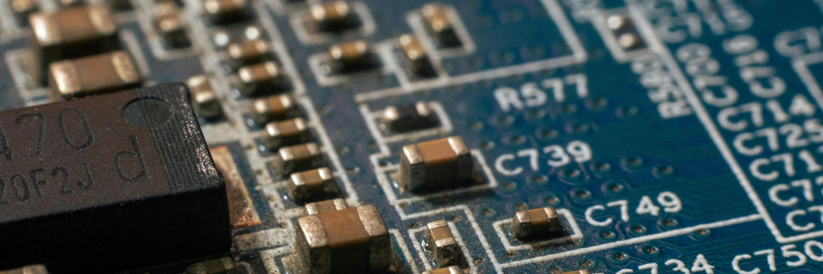
Multilayer PCBs have become an essential component in meeting the complex design requirements of next-generation electronic systems. By offering a unique combination of higher functionality, smaller space, and improved performance, multilayer PCBs enable the design of smaller devices with enhanced capabilities. In this post, we explore several benefits of multilayer PCBs, their applications, key considerations for choosing them, and their growing role in cutting-edge industrial applications.
- Higher Functionality in Smaller Space
One of the most significant advantages of multilayer PCBs is their ability to pack a higher number of electrical circuits into a smaller area. This is particularly important in industries where miniaturization is a key factor, such as in smartphones, wearables, and consumer electronics. Multilayer PCBs:
-
- Enable Compact, Lightweight Designs: By distributing circuits across multiple layers, multilayer PCBs allow engineers to reduce board size without sacrificing performance. This enables the design of smaller, lighter devices while maintaining advanced functionality.
- Support High-Density Interconnect: With multiple layers, multilayer PCBs can support high-density interconnections, enabling complex designs with reduced space. This is essential for modern high-speed computing and data processing systems.
- Improved Electrical Performance
Multilayer PCBs are known for their ability to deliver superior electrical performance, making them ideal for high-frequency and high-speed applications. This improved electrical performance is achieved through several design advantages inherent to multilayer PCB construction, including:
-
- Shorter Signal Paths: By using multiple layers, signal traces can be placed closer together, reducing the distance signals need to travel. This results in faster transmission speeds, lower latency, and overall improved performance.
- Better Signal Integrity: Multilayer PCBs improve signal integrity by providing dedicated planes for power and ground. This helps minimize signal degradation and ensure reliable communication in high-speed circuits.
- Controlled Impedance: Multilayer designs allow engineers to control impedance more effectively, a critical factor in high-frequency applications such as 5G, RF, and microwave systems.
- Enhanced Power Distribution
Efficient power distribution is another key advantage of multilayer PCBs. By incorporating several design strategies, these PCBs can distribute power more evenly and reduce the likelihood of power fluctuations, which can lead to device failures. This is achieved through dedicated layer design and electrical isolation techniques such as:
-
- Dedicated Power and Ground Planes: The ability to integrate separate power and ground layers helps isolate sensitive signal traces from noisy power signals, improving the stability and performance of the entire system.
- Reduced Noise and Ripple: Multilayer PCBs reduce the chances of power ripple and electromagnetic interference (EMI), resulting in more stable and reliable power delivery, which is critical for devices such as automotive electronic control units (ECUs) and medical equipment.
- Reduced EMI & Crosstalk
In modern electronics, electromagnetic interference (EMI) and crosstalk (unwanted signal interference between different circuit traces) are significant concerns. In multilayer PCBs, this interference control is achieved through structural design choices, including:
-
- Better Signal Isolation Through Stacking: The separation of signal layers and power layers in multilayer PCBs ensures better EMC, reducing the risk of signal interference and maintaining the integrity of the electrical signals.
- Increased Reliability & Strength
Multilayer PCBs provide greater mechanical strength and reliability compared to traditional single or double-sided PCBs. This added strength is critical in harsh environments where failure isn’t an option. It is constructed meticulously with:
-
- Strong Multilayer Laminated Structure: The laminated structure of multilayer PCBs enhances their ability to withstand mechanical stress, making them highly reliable for demanding applications such as space electronics and automotive systems.
- Better Thermal Management: Multilayer PCBs offer enhanced thermal dissipation by incorporating dedicated thermal layers or using materials with high thermal conductivity, which prevents overheating.
- Supports Advanced Technologies
Multilayer PCBs are critical for the advancement of modern technologies, particularly those that demand high levels of miniaturization and performance. These PCBs are designed to support;
-
- HDI, Microvias, Fine-pitch Components: Multilayer PCBs enable the use of advanced design features such as microvias and fine-pitch components, making them ideal for high-speed, high-performance applications including 5G infrastructure, RF communications, and high-frequency circuits.
- High-Speed, RF, and Microwave Designs: The compact design of multilayer PCBs makes them a preferred choice for high-speed applications in telecommunications, military, and medical technologies.
Where Multilayer PCBs Solve Critical Design Challenges
Modern electronics face three impossible demands: smaller size, more functionality, higher reliability. Multilayer PCBs answer all three. Here’s where they make the difference.
- When Space is Non-Negotiable: Smartphones and wearables pack processing power, sensors, and communication modules into devices thinner than a pencil. Single-layer boards can’t deliver this density. Multilayer PCBs stack functionality vertically, enabling the pocket-sized technology we take for granted.
- Where Failure Means Lives at Risk: Pacemakers don’t get second chances. Neither do implantable insulin pumps or surgical diagnostic equipment. Medical devices demand circuit boards that function flawlessly for years inside the human body. Multilayer PCBs provide the reliability and miniaturization that make life-saving technology possible.
- In Environments That Destroy Ordinary Electronics: Aerospace and defense systems operate in extreme conditions—vibration, temperature swings, electromagnetic interference. A fighter jet’s avionics or a satellite’s guidance system can’t tolerate signal degradation or component failure. Multilayer PCBs deliver the signal integrity and durability these applications require.
- Driving Industrial Precision: Factory robots, automated quality control systems, and sensor networks coordinate complex operations with millisecond timing. Industrial automation demands PCBs that fit tight spaces while managing multiple communication protocols and power requirements simultaneously.
- Making Vehicles Smarter and Safer: Your car’s ability to brake automatically, maintain lane position, or manage engine performance depends on electronic control units (ECUs) and advanced driver assistance systems (ADAS). These automotive systems process sensor data, execute split-second decisions, and distribute power, all through compact multilayer PCB architectures.
- Keeping the World Connected: 5G towers, data centers, and network routers handle billions of data packets daily. Telecom and networking equipment relies on multilayer PCBs to maintain signal integrity at high frequencies while managing heat dissipation in equipment that runs 24/7 without interruption.
Powering the Future of Electronics with Multilayer PCBs
Multilayer PCBs aren’t just enabling current technology; they’re making future innovations possible. As devices continue shrinking while performance demands escalate, the role of advanced PCB design becomes even more critical. Industries from healthcare to aerospace depend on multilayer PCBs that deliver reliability, performance, and miniaturization in equal measure.
Rigiflex specializes in engineering and manufacturing high-performance multilayer PCBs for demanding applications. From prototype to production, we work closely with engineers to optimize layer stackup, control impedance, manage thermal dissipation, and ensure signal integrity.
Our advanced manufacturing capabilities support HDI designs, microvias, fine-pitch components, and the tight tolerances that modern electronics demand. Contact Rigiflex today to discuss your multilayer PCB requirements. Let’s engineer the circuits that power your innovation.
