PCB manufacturing comprises a variety of processes to produce different types of circuit boards. One of the popular board options provided by most PCB suppliers is multilayer PCBs. The entire manufacturing and assembly processes for these PCB types is extremely interesting. Customers can even learn how to reduce costs by understanding more about multilayer PCB assembly. We provide all the details for you in this post.
Understanding the Multilayer PCB Manufacturing Process
The process of manufacturing multilayer circuit boards is quite straightforward. However, it does require the engineers to pay attention to detail. The following are the manufacturing process steps in brief:
- Front End Tool Data Preparation: The designer prepares the PCB layout using a Computer Aided Design (CAD) system, and creating Gerber files.
- A Photo plotter is used to create an image of the PCB. The image contains information that the machines use to print PCB inner layers from a glass fiber core.
- An alkaline solution is used to etch the inner layers and remove unwanted copper from the PCB image.
- Holes are punched to help align the outer and inner layers.
- All layers are bonded together and via holes are drilled into the PCB to connect the copper layers. Blind and buried vias are created when the PCB design does not connect with all the inner layers.
- A thin layer of liquid copper is used to cover the drilled holes, which are then electroplated.
- The outer layers are etched to remove any residual copper. A layer of tin is applied on top of the liquid copper layer for protection.
- A solder mask is printed on both sides of the board to protect the copper surface.
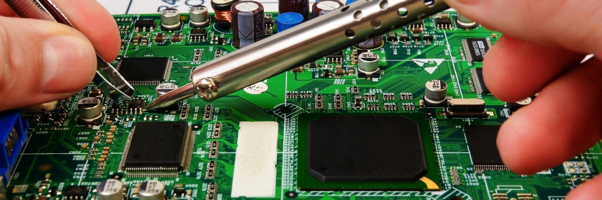
- The PCB components are then soldered onto the board.
- The circuit board is profiled and cut according to the customer’s requirements.
- The board is inspected, and any errors are rectified, before sending for delivery.
Manufacturing Considerations for Multilayer PCBs
Many times, customers ask for unconventional designs, or extra specifications in the final PCB. While this is not impossible, the result of this can lead to higher prices, more manufacturing time, and slower delivery time. Hence, you need to consider the following points when it comes to multilayer PCBs.
- FrontThe right materials should be chosen to support the weight of the multiple layers.
- Layer and board orientation should be followed according to the sequence provided in the diagram.
- Larger geometries will lead to higher prices in terms of the overall PCB quantity.
- Copper used on the inner layers should be at a distance of 10 or 20 mil from the outer edge of the board.
- Antipads should be used to ensure via clearance through the inner layers.
- If any holes or via a barrels are not connected to any inner layers, then ensure that there is clearance of about 15 or 20 mils around holes and barrels.
- All the layers should be registered to particular holes drill in the boards. Also, the registration should remain even when the PCB is subjected to heat or pressure.
The above points are related to ‘tried and true’ designs. By keeping these points in mind, you will be able to create a PCB that can be manufactured in bulk, will not be excessively expensive, and will be delivered on time. If you are looking for Multilayer PCB, or other types, you can contact Rigiflex Technology, Inc.
