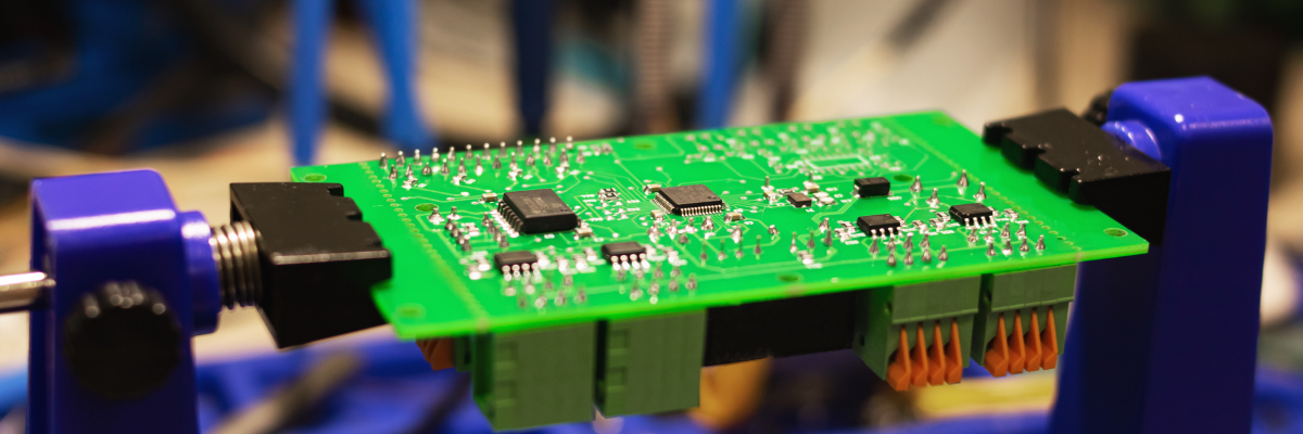
As the demand for performance-driven, high speed, and yet miniature devices grows, printed circuit board (PCB) manufacturing and assembling have gained immense traction as almost all of these products and devices are driven by PCBs. A flawless PCB design is crucial for further processes such as accurate mounting of components, circuits, vias, and so on. Through-hole and surface mount are two widely used techniques for component mounting, vias, and wiring. Vias are a particularly important part of this design, especially in boards with multiple layers, as they are the plated or non-plated holes through which layers of the board can connect via copper traces. They ensure ease of routing and that the boards are manufactured exactly as per the design. But, PCB vias are more than simply interfaces for routing. They must be designed with precise dimensions to comply with industry manufacturability and reliability standards. This post focuses on top PCB vias design rules for circuit board layouts. So, stay tuned.
PCB Vias – Introduction and Types Discussed
Vias stand for vertical interconnect access. They are plated through holes in the circuit board. Vias deliver a route using which thermal and electrical energy moves from one circuit layer to another. Depending on the application requirement, PCB vias can be either drilled by laser or mechanically. They are an essential part of multi-layered PCBs, which are complex to design and manufacture. There are different types of vias in use today. PCB vias design rules for circuit board layouts are different for each of these types.
- Through-hole Vias: This is one of the important types of PCB Vias, in which holes are drilled from the top layer to the bottom. The holes can be either plated or non-plated. Both ends are opened in this type of vias. This enables plating to flow throughout the circuit board.
- Buried Vias: Buried vias are popularly called hidden vias as they are located in the inner region of the board. Thus, there are no paths towards the outer layers. They can be drilled mechanically.
- Blind Vias: They are drilled mechanically from top or bottom. It means blind vias connect the top to the center layer or the external layer to the adjacent layer. The other side of the hole can’t be seen once done with the lamination, hence they are called blind vias.
PCB Vias Design Guidelines for Through-hole, Buried, and Blind Vias
Each PCB via types mentioned above have their specific designing rules. This section describes the same.
Through-hole PCB Vias
- Through-hole PCB vias demand a drill pad on every circuit board layer. The drill pad should be tiny but large enough for the drill being used. Additionally, the thru-hole via requires a standard anti-pad on the plane layers of the board to avoid short circuits between neighboring holes.
- Another important design rule for through-hole PCB vias is to choose appropriate via size. The sizes of via should be chosen considering the aspect ratio of the drilled hole in terms of the board thickness.
- In the multi-layer circuit board, if a through-hole via can connect high-speed signals between the first two layers, the remaining or unused via barrel may act as an antenna. However, this may create signal integrity issues. OEMs overcome this problem through back drilling. However, this process increases overall fabrication costs. The best practice is to use blind and buried or micro vias to improve the board performance.
- Through-hole vias can be filled or covered if required. For this, the PCB designer provides specific instructions to the fabricator.
Buried PCB Vias
- As discussed earlier, buried vias connect internal layers of the circuit boards, which have no contact with the outer layers.
- The hole should be defined as a separate drill file for a single connection.
- The aspect ratio should be 1:12 or larger.
- The small hole determines the overall depth and maximum distance between the inner layers and respective outer layers.
- Buried vias are mainly useful for PCBs with dense routing.
Blind PCB Vias
- Blind vias are mechanically drilled, thus they have similar drill size limitations as through-hole. They allow extra routing channels above or below via in-the-layer stack-up. This capability gives an advantage to blind vias compared to through-hole.
- Like buried, in blind vias, each hole must be defined as a separate drill line.
- The aspect ratio should be 1:1 or larger.
- This type of vias is built sequentially, meaning the circuit board layers are drilled and plated before being bonded together. Thus, PCB designers should take extra care and only use them when required.
The aforementioned PCB vias design rules for circuit board layouts not only increase the density but also bring down the overall production cost. PCB manufacturing processes have eased with the advancement in their high-density designs. But, the requirement sharing should be done properly to get the right PCB vias in the design. If your next electronics project involves PCBs, then the above guidelines may serve your purpose. If in doubt, you must consult an experienced PCB manufacturer and service provider for the best possible solution. With vast years of experience and highly skilled employees, Rigiflex Technology utilizes reliable vias filling processes for designing and manufacturing high-density PCBs. They offer end-to-end PCB manufacturing and assembly solutions.
