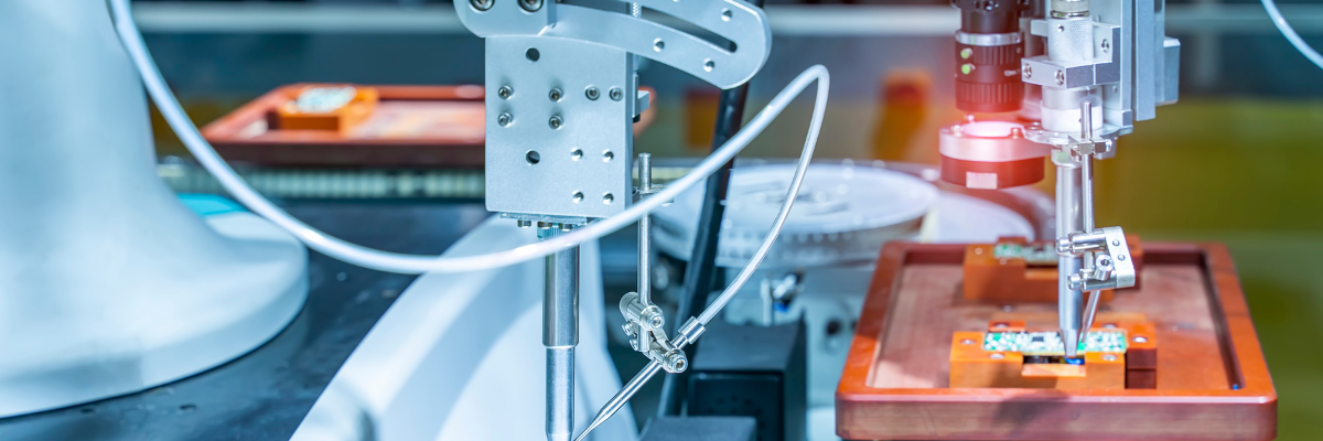
PCBs are the core of most electronic and electromechanical devices used today. They are the backbone of the devices in which they are embedded because their functionality is highly reliant on the design, operation, and accuracy of these PCBs. The demand for miniature yet complex devices has gone up over the last few years, this subsequently has increased the need for multi-layer PCBs with several components. The shrinking of these devices has made the circuit board design and layering complex. These layers, along with the mounted components, should be rightly arranged. This post focuses on essential guidelines for standard PCB layer stack-up designs. So, stay tuned.
Importance of Standard PCB Layer Stack-up
Different materials are used in PCB manufacturing, such as metal, fiber, glass, and so on. Each of them has an insulating and copper layer. Nowadays, multi-layer PCBs are much required owing to devices with multiple functionalities. This demands multiple layers to be embedded in a single device. Extra efforts are required while layering to avoid damage to any of these coatings or mounted components. Thus, organized stacking is of utmost importance. The following pointers help you understand this in a better way.
- Standard PCB layer stack-up increases the processing speed which results in enhanced device functionality.
- Proper layering makes it possible to make compact-sized boards by placing all the required components and circuits on a single board.
- Proper layering also reduces the crosstalk, external noises, radiation, and other possible interferences within the layers.
- Well-stacked circuit boards can be easily fitted and shipped out. This helps reduce the overall packaging costs.
Proven and Easy-to-Follow Guidelines for Standard PCB Layer Stack-up
Standard PCB layer stack-up can be implemented by following certain guidelines in accordance with the application and its requirements. Here is a list of a few important ones.
- Standard PCB layer stack-up highly relies on the number of layers present in the design. This includes considering signal, ground, and power layers. The number of signal layers that need to be used changes in accordance with the circuit board applications. For example, low-power applications may require minimum layers compared to high-speed signal levels. Ensure you use appropriate signal types on inner layers and do not mix them. With the following pin density formula, it is possible to get an accurate layer count for most PCBs.
PIN Density = Circuit Board Area/Total Number of Pins/14
Once done with the calculation, you can check a readily available lookup table to determine the number of layers.
- Sequential layer arrangement is the key aspect of the stack-up design. One of the key parameters that designers need to understand before routing is arranging high-speed signal layers based on the thickness of microstrips. The tight coupling between the layers and components is possible by placing signal layers below the power plane. For precise layer arrangements, ensure minimal spacing between power and ground layers. Additionally, avoid placing two signal layers adjacent to each other. Limit the number of lamination steps as they become expensive and time consuming.
- Another important consideration for standard PCB layer stack-up is the signal layer thickness, which should be established in conjunction with determining thicknesses for core and prepreg. Different PCB material types have different standard thicknesses, mechanical, electrical, and thermal properties. It is important to consider these pointers while selecting the material type.
- PCB stack-up design is completed with the routing of traces, which includes what types of vias to use, where to implement vias, copper weights, and so on. One may consult industry experts for all such specifications of stack-up designs.
Along with the PCB stack-up design guidelines, it is crucial to consider your application requirements. If you plan to incorporate PCBA in your products, partnering with a reliable PCB manufacturer and assembly service provider is always advisable. Rigiflex Technology stands tall among its other competitors. With vast years of industry experience and expertise, the company offers customized and end-to-end PCBA solutions.
