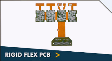
Rigid-flex PCBs are an integral part of electronic applications because they combine rigid and flexible technologies. These printed circuit boards feature several layers of flexible circuit substrates attached to a rigid board. As the name suggests, the rigid-flex circuit boards offer both – flexibility and rigidity, which are important requirements in several applications. At Rigiflex Technology, Inc., we provide rigid-flex PCBs in different specifications and unique designs such as a 16-layer rigid-flex PCB with 12-layer flex PCB bookbinding.
The circuit bookbinding helps increase the length of the circuit in an outward direction from the bend radius. This length addition is influenced by different factors such as the tightness of the bend or number of layers of the circuit. This method helps avoid the bending of the circuit in different directions and channelizes it to only one direction. It also releases tension from the different circuit layers, and helps prevent buckling at the bend radius.
We can provide 16-layer rigid-flex printed circuit boards with 12-layer flex PCB bookbinding in different specifications. These PCBs are made from a wide range of board materials such as FR4, Rogers Ultralam 2000, Rogers RO4350, Rogers RO4003, black FR4, Arlon AR350, and more. We use different types of connectors to terminate the extreme ends of flexible PCBs. In many cases, we also use stiffeners for termination. Thermo Set and PSA based aluminum, FR4, stainless steel, and polyamide are some of the common stiffeners used by us. We understand that the current requirements of these 16-layer rigid-flex PCBs will vary across different applications. Copper thickness is one of the important factors contributing to the current carrying capacity of these PCBs. Knowing this, we design these PCBs in different copper thicknesses from 1 Oz to 5 Oz for outer layers, and from 0.5 Oz to 4 Oz for inner layers. The copper traces are masked with a thin lacquer-like polymer layer to protect it against oxidation. We provide these PCBs in different solder mask colors such as green/green, matte white, black/black, matte clear, blue top and bottom mix, red one or both sides mix, and so on.
Over the years, we have invested in technologies and expertise, which allows us to take complex printed circuit board projects, and complete them in the shortest turnaround times. Do you have any complex rigid-flex circuit board design in mind? Our experts will work with you to understand your requirements, while suggesting you the right materials and specifications. At Rigiflex, our objective is delivering you the highest-quality products at competitive prices.
| 16 Layer Rigid-Flex |
| Specifications |
Technology |
|
|
| FR4 (Tg – 135C, 145C, 170C) |
| Rogers Ultralam 2000 |
| Rogers RO4350 |
| Rogers RO4003 |
| Polyimide |
| Teflon |
| Black FR4 |
| Arlon AR350 |
| Getek Copper Clad Thermal Substrates |
| Hybrid (Rogers and FR4) BT Epoxy |
| Nelco 4013 |
| Metal Core Materials |
|
|
|
| Thermo Set and PSA Based Aluminum |
| FR4 |
| Stainless Steel |
| Polymide |
|
|
|
| 2 Layer – Min .005″ Max .250″ |
| 4 Layer – Min .015″ Max .250″ |
| 6 Layer – Min .025″ Max .250″ |
| 8 Layer – Min .031″ Max .250″ |
| 10 Layer – Min .040″ Max .250″ |
| 12 Layer – Min .047” Max .250” |
| 14 Layer – Min .054″ Max .250″ |
| 16 Layer – Min .062″ Max .250″ |
| 18 Layer – Min .093″ Max .250″ |
| 20 Layer – Min .125″ Max .250″ |
| 22 Layer – Min .125″ Max .250″ |
| >24 Layer – Min .125″ Max .250″ |
|
|
|
Min .0025″ |
| Maximum PCB Size |
| 2 Layer 20″ x 28″ |
| Mulitlayer 16″ x 26″ |
|
| Minimum Conductor Space |
0.003″ |
| Minimum Conductor Width |
0.003″ |
| Minimum Drill Hole Size |
0.006″ |
| Finish Plating / Surface Finishes |
| HASL – Leaded Solder Tin/Nickel |
| HASL – Lead Free Solder |
| Electroless Soft Gold |
| Wire Bondable Soft Gold |
| Nickel Flash Gold |
| Electroless Nickel |
| Immersion Gold OSP |
| Electrolytic Nickel /Hard Gold and Selective Gold |
| Immersion Silver |
| Immersion Tin |
| Carbon Ink |
| ENIG |
|
| Finished Copper – Outer Layers |
| 1oz Cu – Min .004″ Trace/Space |
| 2oz Cu – Min .005″ Trace Space |
| 3oz Cu – Min .008″ Trace/Space |
| 4oz Cu – Min .010″ Trace/Space |
| 5oz Cu – Min .012″ Trace/Space |
|
| Finished Copper – Inner Layers |
| .5oz Cu – Min .004″ Trace/Space |
| 1oz Cu – Min .005″ Trace/Space |
| 2oz Cu – Min .006″ Trace/Space |
| 3oz Cu – Min .010″ Trace/Space |
| 4oz Cu – Min .012″ Trace/Space |
|
| Inner Layer Clearances |
| Min .008″ |
| Minimum Finished Hole Size |
| Final Thickness 062″ – .006” Hole Final Thickness .150″ – .014″ Hole |
| Final Thickness .093″ – .010″ Hole Final Thickness .200″ – .018″ Hole |
| Final Thickness .125″ – .012″ Hole Final Thickness .250″ – .020″ Hole |
|
| Gold Fingers |
| Per IPC-SM-840 |
| LPI Soldermask |
| Peelable Soldermask |
|
| Solder Mask Colors |
| Green/Green |
| Matte White |
| Black/Black |
| Matte Clear |
| Blue Top and Bottom Mix |
| Red One or Both Sides Mix |
|
| Silkscreen Type |
| Thermal Cure Epoxy Ink |
| LPI Ink |
|
| Silkscreen Colors |
| White |
| Black |
| Yellow Top and Bottom Mix |
| Red One or Both Sides Mix |
| Blue |
|
| CNC Functions |
| Scoring Edge to Edge Plated Counter bores |
| Skip Scoring – .250″ Spacing Milling |
| 30 or 60 Degree Score Angle Blind and Buried Vias |
| 30 to 100 Degree Countersink Controlled Z Axis Route |
| 15 to 45 Degree Gold Finger Bevel Castellated Barrels |
| Counterbores Offset or Recessed Beveling |
| Plated Countersinks |
|
| Other PCB Services |
| Blind and Buried Vias |
| Plated Slots Specified Dielectric |
| Tented Vias Controlled Impedance |
| Solder mask Plugged Vias Via Caps (Solder Mask) |
| Conductive Filled Vias |
|
| Quality / Testing |
| Inspect to IPC Class III Continuity Resistance – 10 to 20 Ohms |
| Net List Test per IPC-356D Isolation Resistance – 2 to 30 Megaohms |
| Test Voltage – 100 to 250 Volts Minimum SMT Pitch 0.5 mm |
|
| Tolerances |
| PTH Hole Size – +/- .002″ |
| Front to Back – +/- .002″ |
| NPTH Hole Size – +/- .001″ |
| Solder Mask – +/- .002″ |
| Tooling Holes – +/- .001″ |
| Hole to Pad – +/- .005″ |
|