LOGO
(714) 688-1500   pcboards@rigiflex.com

Flex & Rigid-Flex PCBs.. 1-5 Day Quick Turn

FLEXIBLE PCBS
RIGID-FLEX PCBS
RIGID PCBS

Superior & Trusted Flexible, Rigid-Flex & Rigid PCBs for Over 25 years

18 Layer Rigid-Flex PCB with 12 Layer Flex PCB with Air Gap

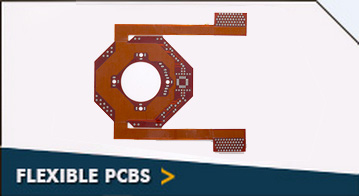
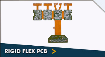
Rigiflex is known for creating flawless flexible printed circuit boards in par with the requirements of several industries. So far, we have handled hundreds of thousands of PCB projects, and is capable to take your application from concept to production. We are committed to delivering time-critical and high performance flexible circuit boards, whilst maintaining good flex-circuit stability and lifespan. Our range of 18 layer rigid-flex PCB with 12 layer flex PCBs with air gaps is also the result of expert designing and manufacturing excellence. Rigiflex boasts several years of experience in developing these reliable flexible circuit boards for applications in automotive, medical, industrial, aerospace, military, and telecommunications, among several others.

There existed a high chance of dielectric breakdown in multilayered, high voltage PCBs, which was a headache for the PCB manufacturers worldwide. Rigiflex, with its engineering experience and expertise, has designed 18 layered rigid flex PCBs with air gaps, and thus tackled the issue. These rigid flex printed circuit boards are designed with a minimum clearance distance between the air gaps. We strictly ensure that that the air gap is not less than 10 mm. This helps to prevent any type of dielectric breakdown in the PCB. The air gaps act as reinforced insulation between PCB components, preventing any kind of hazardous voltage. The gaps also help to prevent the accumulation of dust or dirt on the PCB surface, whilst helping maintain the service life of the PCB.

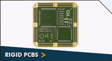
At Rigiflex, 18 layer rigid-flex PCB with 12 layer flex PCBs are produced in a wide range of board materials. A few amongst them include FR4 (Tg – 135C, 145C, 170C), Rogers Ultralam 2000, Polyimide, Teflon, Black FR4, Arlon AR350, Getek Copper Clad Thermal Substrates, and Hybrid (Rogers and FR4) BT Epoxy. Also, we use Thermo Set and PSA Based Aluminum, FR4, Stainless Steel, and Polymide stiffeners. Solder mask colors such as green/green, matte white, black/black, matte clear, blue top and bottom mix, and red one or both sides mix are used in assembling18 layer rigid-flex PCB with 12 layer flex PCBs.

At Rigiflex, we possess capabilities in assembling PCBs with blind and buried vias, plated slots specified dielectric, tented vias controlled impedance, solder mask plugged vias, via caps (solder mask), and conductive filled vias. Since all the PCBs are vacuum packed in plastic bags before shipping, they will reach safely at the customers’ doorsteps without any damage during the transit.

18 Layer Rigid-Flex
Specifications Technology
Board Materials
FR4 (Tg – 135C, 145C, 170C)
Rogers Ultralam 2000
Rogers RO4350
Rogers RO4003
Polyimide
Teflon
Black FR4
Arlon AR350
Getek Copper Clad Thermal Substrates
Hybrid (Rogers and FR4) BT Epoxy
Nelco 4013
Metal Core Materials
Stiffeners
Thermo Set and PSA Based Aluminum
FR4
Stainless Steel
Polymide
Final PCB Thickness
2 Layer – Min .005″ Max .250″
4 Layer – Min .015″ Max .250″
6 Layer – Min .025″ Max .250″
8 Layer – Min .031″ Max .250″
10 Layer – Min .040″ Max .250″
12 Layer – Min .047” Max .250”
14 Layer – Min .054″ Max .250″
16 Layer – Min .062″ Max .250″
18 Layer – Min .093″ Max .250″
20 Layer – Min .125″ Max .250″
22 Layer – Min .125″ Max .250″
>24 Layer – Min .125″ Max .250″
Core Thickness
Min .0025″
Maximum PCB Size
2 Layer 20″ x 28″
Mulitlayer 16″ x 26″
Minimum Conductor Space 0.003″
Minimum Conductor Width 0.003″
Minimum Drill Hole Size 0.006″
Finish Plating / Surface Finishes
HASL – Leaded Solder Tin/Nickel
HASL – Lead Free Solder
Electroless Soft Gold
Wire Bondable Soft Gold
Nickel Flash Gold
Electroless Nickel
Immersion Gold OSP
Electrolytic Nickel /Hard Gold and Selective Gold
Immersion Silver
Immersion Tin
Carbon Ink
ENIG
Finished Copper – Outer Layers
1oz Cu – Min .004″ Trace/Space
2oz Cu – Min .005″ Trace Space
3oz Cu – Min .008″ Trace/Space
4oz Cu – Min .010″ Trace/Space
5oz Cu – Min .012″ Trace/Space
Finished Copper – Inner Layers
.5oz Cu – Min .004″ Trace/Space
1oz Cu – Min .005″ Trace/Space
2oz Cu – Min .006″ Trace/Space
3oz Cu – Min .010″ Trace/Space
4oz Cu – Min .012″ Trace/Space
Inner Layer Clearances
Min .008″
Minimum Finished Hole Size
Final Thickness 062″ – .006” Hole Final Thickness .150″ – .014″ Hole
Final Thickness .093″ – .010″ Hole Final Thickness .200″ – .018″ Hole
Final Thickness .125″ – .012″ Hole Final Thickness .250″ – .020″ Hole
Gold Fingers
Per IPC-SM-840
LPI Soldermask
Peelable Soldermask
Solder Mask Colors
Green/Green
Matte White
Black/Black
Matte Clear
Blue Top and Bottom Mix
Red One or Both Sides Mix
Silkscreen Type
Thermal Cure Epoxy Ink
LPI Ink
Silkscreen Colors
White
Black
Yellow Top and Bottom Mix
Red One or Both Sides Mix
Blue
CNC Functions
Scoring Edge to Edge Plated Counter bores
Skip Scoring – .250″ Spacing Milling
30 or 60 Degree Score Angle Blind and Buried Vias
30 to 100 Degree Countersink Controlled Z Axis Route
15 to 45 Degree Gold Finger Bevel Castellated Barrels
Counterbores Offset or Recessed Beveling
Plated Countersinks
Other PCB Services
Blind and Buried Vias
Plated Slots Specified Dielectric
Tented Vias Controlled Impedance
Solder mask Plugged Vias Via Caps (Solder Mask)
Conductive Filled Vias
Quality / Testing
Inspect to IPC Class III Continuity Resistance – 10 to 20 Ohms
Net List Test per IPC-356D Isolation Resistance – 2 to 30 Megaohms
Test Voltage – 100 to 250 Volts Minimum SMT Pitch 0.5 mm
Tolerances
PTH Hole Size – +/- .002″
Front to Back – +/- .002″
NPTH Hole Size – +/- .001″
Solder Mask – +/- .002″
Tooling Holes – +/- .001″
Hole to Pad – +/- .005″

Quick Contact

All Fields are Mandatory (*)

Capcha

Fourbox

Need it quick? That is our speciality!